Layertronics – Controlling the layer localization of topologically protected states in bilayer graphene
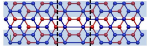
Fig 1. Domain wall separating two stackings of bilayer graphene.
A stacking domain wall in bilayer graphene is a boundary separating two regions with opposite stackings, i.e., AB and BA. When gated, it reveals having topologically protected states, that along the domain occur to be very robust conducting channels. In previous research, we found firstly that the number of topologically protected states in corrugated and defectless domain walls is constant and equal to two [1]. We also showed that atomic-scale defects in the domain wall may strongly affect the gapless states. Even their number in the gap, which reflects the number of open conductance channels, change with the gate voltage polarization [2]. The origin and exact localization of such states, however, require a more detailed study.

Fig 2.Layer-resolved local density of states as a function of the magnitude of the gate voltage. Note that the two topologically protected states in the gap exchange layer localization with the gate voltage value.
In a recent work we investigate these gapless states for defectless domain walls, using atomistic lattice models, which permit to study their origin by following the formation of carbon bonds between layers. More importantly, we analyze the layer localization and show that it depends on the ratio of the gate potential to the interlayer hopping. Two different regimes are thus defined for small and large gate voltages that may open a route for the use of topologically protected states in practical devices. The control of the carriers localization in distinct layers along domain walls opens the possibility for the design of ‘layertronic’ devices, which could be exploited in addition to other degrees of freedom, like valley, spin and charge, in graphene-based electronics.
[1] Pelc et al. Phys Rev. B 92, 085433 (2015)
[2] Jaskólski et al. Nanoscale 8, 6079 (2016)