Achieving Record High Room Temperature Resistance Switching in Ferroelectric-Gated Mott Transistors
An experimental team led by Xia Hong at University of Nebraska–Lincoln reports a record of ferroelectric-gated Mott transistors, showcasing a high resistance switching ratio of 38,440% at room temperature. Based on first-principles calculations, Yue-Wen Fang at CFM emphasized that the driving force behind achieving high resistance switching is the interface charge transfer.
Over the past two decades, there has been significant research on the device concept of ferroelectric field-effect transistors based on Mott insulator channels, known as Mott FeFETs. Mott FeFETs have energy-efficient memory and logic applications, as the intrinsically high carrier density of the correlated material (1022-1023/cm3) promises sub-nanometer size scaling beyond the fundamental limit of semiconductor technology. However, despite the potential advantages, challenges arise from the close-to-metallic carrier density, particularly in achieving substantial conduction modulation in the channel with a solid-state gate. Previous studies have concentrated on single-layer correlated channels, yet these efforts have only resulted in moderate resistance switching at room temperature. This limitation is attributed to the intricate interplay of charges, influencing both the magnitude and retention of field-effect modulation. Addressing these challenges is crucial for unlocking the full potential of Mott FeFETs in practical applications.
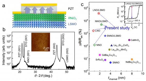
Figure 1. (a) Device schematic. (b) XRD θ−2θ scan taken on a PZT/NdNiO3 (NNO)/La0.67Sr0.33MnO3 (LSMO) heterostructure deposited on (001) SrTiO3 (STO) substrate. Inset: AFM topography image of the sample. (c) Maximum ΔR/Ron vs. thickness of channel (tchannel) achieved in various correlated oxide materials.
In this work the researchers exploited ferroelectric PbZr0.2Ti0.8O3 (PZT)-gated rare earth nickelates RNiO3 (R = La, Nd, Sm) as a model system to show that a record high nonvolatile resistance switching ratio of 38,440% can be achieved at 300 K by inserting an ultrathin charge transfer layer La0.67Sr0.33MnO3 (LSMO). The structure model of such a heterostructure is schematically shown in Fig. 1a. The researchers used magnetron sputtering techniques to deposite epitaxial PZT/RNiO3 and PZT/RNiO3/LSMO heterostructures on mixed termination (001) LaAlO3 and SrTiO3 substrate (XRD and the atomic force microscopy of this heterostructure is available at Fig. 1b).
A systematic comparison between RNiO3 single-layer channels and RNiO3/LSMO bilayer channels shows that the resistance switching ratio increases exponentially with decreasing channel thickness till the channel becomes electrically dead, while the composite channels with the same total channel thickness exhibit up to three orders of magnitude higher resistance modulation. In particular, the LNO/LSMO bilayer channel enables the realization of highest switching ratio among all the existing studies (see Fig. 1c). The drastically enhanced field effect has been attributed to a tailored carrier density profile in the RNiO3 channel due to the interfacial charge transfer with the ferromagnetic LSMO, as shown by the density functional theory (DFT) calculations about the charge transfer at the interfaces in Fig. 2.
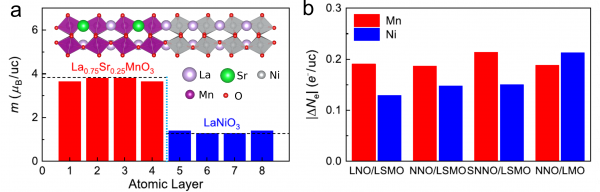
Fig. 2 (a) Layer projected magnetic moments of transition metal ions used for analyzing the charge transfer in LSMO/LNO heterostructure. (b) Charge transfer values at different interfaces.
The device model presented in this study capitalizes on the competitive device parameters, scalable epitaxial growth, and voltage-controlled nature. It holds the potential to seamlessly integrate complex oxides with the Silicon platform. As a result, it provides a robust material strategy for advancing next-generation high-density, low-power nanoelectronics, and spintronics.
Reference: “Record high room temperature resistance switching in ferroelectric-gated Mott transistors unlocked by interfacial charge engineering”
DOI: 10.1038/s41467-023-44036-x