Atomically-precise texturing of hexagonal boron nitride nanostripes
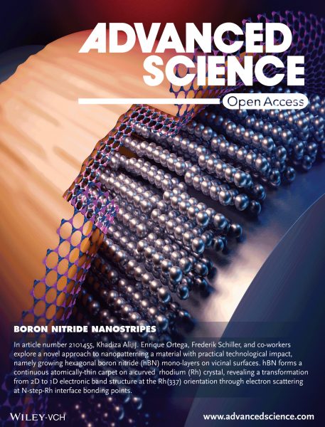
Featured on the cover of Advanced Science, the STM image and a model of how hBN covers a cylindrical Rh crystal approx. 10° away from the (111) direction.
Monolayer hexagonal boron nitride (hBN) can be epitaxially grown on vicinal rhodium (Rh) surfaces using a Rh curved crystal for a systematic exploration, which produces a periodically textured, nanostriped hBN carpet that coats Rh(111)-oriented terraces and lattice-matched Rh(337) facets with tunable width. The electronic structure reveals a nanoscale periodic modulation of the hBN atomic potential that leads to an effective lateral semiconductor multi-stripe.
Since the discovery of graphene, a wide diversity of atomic-layer-thick, two-dimensional (2D) materials with varied properties have emerged. Of particular interest are those that exhibit semiconducting behavior, such as hexagonal boron nitride (hBN). hBN is isoelectronic to graphene and has also a honeycomb lattice formed by alternating nitrogen and boron atoms, but in contrast to the semimetallic graphene, its band structure presents some characteristics that makes it particularly attractive for applications in microelectronics, either alone or in combination with other 2D materials, such as graphene. Furthermore, hBN is structurally robust and chemically inert. Although hBN flakes may be obtained by mechanical exfoliation of bulk crystals, a single hBN monolayer can be readily synthesized on metal surfaces, leading to structurally and chemically robust substrates that frequently exhibit nanoscale patterns. This makes hBN-covered metals excellent platforms to achieve functional interfaces with atoms, molecules, and aggregates, as well as to develop hybrid 2D materials, such as twisted van der Waals stacks or 2D heterostructures. The latter hold a great potential for atomically thin circuitry, such as superstructures formed with isostructural graphene, which are optimal to engineer gaps and doping, as well as to tune and enhance spin scattering.
However, this is easier said than done. Exploiting fine hBN-based nanostructures requires structural quality down to the atomic scale and precise lateral nano-structuration and integration with other two-dimensional materials, which lies beyond current lithographic capabilities. The bottom-up vapor growth is the alternative, which also works for 2D hybrids, although general procedures to control shape, size, and spatial order of surface phases are still lacking.
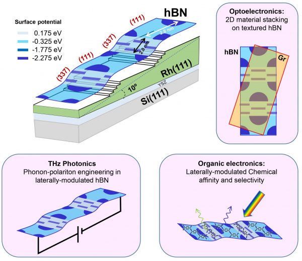
Figure: Lateral nanopatterning of hBN through epitaxial growth. The concept of the study of vicinal hBN/Rh interfaces is presented. CVD growth of hBN induces periodic (111)/(337) faceting of the Rh substrate. The hBN monolayer uniformly coats the faceted substrate, defining an effective lateral hBN/Rh heterointerface with periodic surface potential texturing. Using commercial Rh(111) films, one could exploit such chemical and electronic modulation of hBN to explore phonon–polariton THz excitations, selective growth of optically-active molecules, and vertical stacking with other 2D materials.
Now, a team of researchers from CFM and other collaborating institutions has found a working disruptive approach: imprinting the lateral pattern of an atomically stepped one-dimensional template into a hBN monolayer. The researchers demonstrate the bottom-up synthesis of nanostriped hBN heterostructures with atomically sharp interfaces. The idea was to follow the standard chemical vapor deposition growth route, using rhodium (Rh) vicinal surfaces as one-dimensional (1D) templates. In practice, hBN was epitaxially grown on Rh surfaces using an Rh curved crystal for a systematic exploration, which produces a periodically textured, nanostriped hBN carpet that coats Rh(111)-oriented terraces and lattice-matched Rh(337) facets with tunable width.
Thus, a 1D lateral hBN (111)/(337) heterostructure arises, featuring defect-free boundaries and significant band offsets. The resulting electronic structure reveals a nanoscale periodic modulation of the hBN atomic potential that leads to an effective lateral semiconductor multi-stripe.
Since size tunability of phases can be gained by selecting the Rh vicinal plane, a variety of new possibilities is opened by this discovery. For example, the hBN (111)/(337) faceted system could be used as a model platform to mold and probe 1D phonon–polariton excitations in the THz regime to achieve selective growth of atoms, aggregates, and molecular adsorbates for organic optoelectronics and catalysis, or to tailor the 3D stacking with other 2D materials, such as graphene.