Femtosecond laser direct inscription of 3D photonic devices in Er/Yb-doped oxyfluoride nano-glass ceramics
The present work demonstrates the potential of transparent oxyfluoride nano-glass ceramics co-doped with Er3+/Yb3+ ions for the integration of 3D photonic devices by femtosecond laser inscription in the low repetition-rate regime (1 kHz). The results suggest that this target material is an excellent host for the integration of active photonic devices.
The use of ultrashort laser pulses for the inscription of optical waveguides in transparent dielectrics has attracted great attention since the first demonstration due to the intrinsic properties of the technique; the fabrication is direct and can be applied to almost any transparent dielectric, it does not require any specific sample preparation and, more remarkably, it allows the implementation of 3D structures. Among the different substrates used for waveguide inscription by femtosecond laser irradiation, oxifluoride nano-glass ceramics containing rare-earth doped fluoride nanocrystals combine the good mechanical and chemical stabilities of oxide glasses with the low phonon energy of fluoride crystals, thus being of great interest in the operation of active devices.
This collaborative work carried out by the groups led by Javier Vázquez de Aldana (University of Salamanca), Alicia Durán (ICV-CSIC) and Rolindes Balda (CFM, UPV/EHU), demonstrates the potential of transparent oxyfluoride nano-glass ceramics co-doped with Er3+/Yb3+ ions for the integration of 3D photonic devices by femtosecond laser inscription. The fabrication is not critical, finding a wide range of irradiation conditions (pulse energy and scanning velocity) in which guiding structures are produced supporting high-quality modes. The technique of multi-scan inscription was successfully applied to tailor the refractive index profile of the waveguides, obtaining multimodal structures. The suitability of the glass-ceramics as substrate for the integration of complex photonic elements was demonstrated by implementing several splitter designs, both 2D and 3D (Figure 1, left column). The modal profiles at output preserved the single mode behavior at 633 and 800 nm (see normalized intensity for 800 nm in the Figure, central column). The results demonstrate the optimum behavior of Er3+/Yb3+ oxyfluoride nano-glass ceramics as a host material for the integration of complex 3D active photonic circuits by femtosecond laser irradiation.
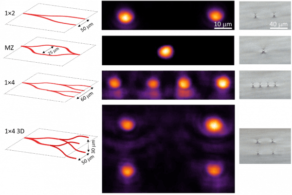
Figure: Scheme of the implemented photonic elements (left column), normalized near-field modal profiles at 800 nm (central column), and microscopic pictures of the output facet (right column). From top to bottom, 1×2 splitter, Mach-Zehnder interferometer, 1×4 splitter (2D), and 1×4 splitter (3D).