Electronic transport in planar atomic-scale structures measured by two-probe scanning tunneling spectroscopy
Miniaturization of electronic circuits into the single-atom level requires novel approaches to characterize transport properties. Since its invention by Binnig et al. in 1982, the scanning tunneling microscope (STM) is regarded as the method of choice for real-space imaging of the electronic structure of conducting surfaces with picometer resolution. Single-probe STM is also a spectroscopic tool, able to locally probe electronic surface states as
a function of the bias voltage in the scanning tunneling spectroscopy (STS) mode. Furthermore, the precision reached in approaching the STM tip apex toward the surface permits for a controlled electronic contact with a single surface atom or molecule.

Figure 1: Artistic view of the 2P-STM operating on Ge(001)-c(4×2). White lines represent electrons transmitted from one tip to the other through the quasi-one-dimensional surface states.
However, direct determination of the electronic transport properties of a planar atomic-scale wire or circuit lies beyond the single-probe approach. Such characterization requires fabricating metal contacts with high precision, which is usually a challenge. An attractive alternative is the use of multi-probe STM. This method offers high control on the position and geometry of the contacts between the probes and the nanoscale system. But the downscaling of multiprobe instruments toward the atomic level, i.e., where all STM tip apex positions are controlled at the atomic scale, meets many technical obstacles. Although two-probe STM (2P-STM) experiments have been proposed already in the nineties, practical implementations of those propositions were not feasible. The main obstacle was the insufficient stability that caused a lack of both atomic precision in relative probe-to-probe positioning and picometer precision in probe-to-sample contact determination. In fact, only recently 2P-STM experiments have reached the required atomic precision in contacting structures on a surface, however no experimental protocols for extracting transport properties of atomic structures from such experiments had been reported.
An international team of researchers, including members from CFM and DIPC, used for the first time a 2P-STM/STS with probes operating in tunneling conditions over the same atomic- scale system to extract detailed information of in-plane electronic transport.
They introduced a new method for the determination of the transconductance and demonstrate how it captures energy-resolved information about electronic transport through the unoccupied states from the anisotropic germanium (001) surface. Combining the new experimental protocol with state-of- the-art first-principles calculations they showed that 2P-STS brings information about coherent hot electrons transport in quasione-dimensional surface states of germanium (001). The Ge(001) surface consists of buckled Ge dimers forming well-separated parallel rows.
The existence of surface dangling bonds introduces additional unoccupied states within the band-gap of the bulk Ge electronic structure. Importantly, weak interactions between adjacent rows result in strong anisotropy of this band structure. Consequently, the reconstructed dimer rows on the bare Ge(001) surface form a series of parallel
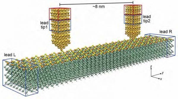
quasi-1D wires. In the experiment, electrons injected from one STM tip are collected at a different location at a nanometric distance (down to 30 nm). This was theoretically modeled by a system composed of a twelve-layer Ge(001)-c(4×2) slab contacted by Au tips (Fig. 1). On this selfconsistent 4-terminal treatment, two Ge electrodes were connected at each slab termination and other two at the Au model tips. A remarkable agreement was found between the calculated transmis- sion function and the experimental transconductance spectra. The sequential opening of two transport channels within the quasi-one-dimensional Ge dimer rows in the surface gives rise to two distinct resonances in the transconductance spectroscopic signal. These breakthrough simulations also elucidated the transport directionality of the injected hot electrons, revealing a transition from 2D to quasi-1D coherent transport regime. This work demonstrates that complex experiment setups combined with advanced calcu- lations can provide new insights into transport properties at the nanoscale. The presented techniques are promising and applicable to characterize the quantum transport in 2D materials in general (graphene and beyond). In contrast to standard metal contacts, e.g., fabricated by lithographic techniques, the use of 2P-STM enables a precise adjustment of individual atomic contacts and their resistances, allowing to access the system’s intrinsic transport properties, disentangling them from those of the contacts and leads.

Figure 2: First-principles transport simulations for the two-probe experiments, represented by a four-terminal setup. The electrode regions are highlighted by blue boxes, two of them located at each Ge(001)-c(4×2) slab terminations and the other two at each Au model tip.


