Existence of nontrivial topologically protected states at grain boundaries in bilayer graphene: signatures and electrical switching
In this work it is discovered that in gated bilayer graphene, gap states with topological origin may be present despite having stacking boundaries, which introduces atom-size defects that cause mixing between sublattices. Furthermore, the number of gap states depends on the sign of the gate voltage applied, a fact of interest for the design of future electronic devices.
The appearance of gapless states in stacking domain walls can be much more common in bilayer graphene. They are also shown in unexpected geometries, for instance, at grain boundaries with atomic-scale topological defects. We focus on bilayer graphene in which one of the layers contains a line of octagon—double-pentagon defects. This work demonstrates that even with pentagonal defects mixing graphene sublattices, gap states are preserved. It is however observed that both topological and defect-originated states strongly hybridize, in a game mainly determined by the gate voltage polarization. Thus, unlike previous predictions, the number of gap states changes by inverting the gate voltage sign, which originates an asymmetric conductance along the grain boundary under gate reversal. The authors expect that this effect, linked to defect states, should be detectable in transport measurements and could be exploited in electrical switches.
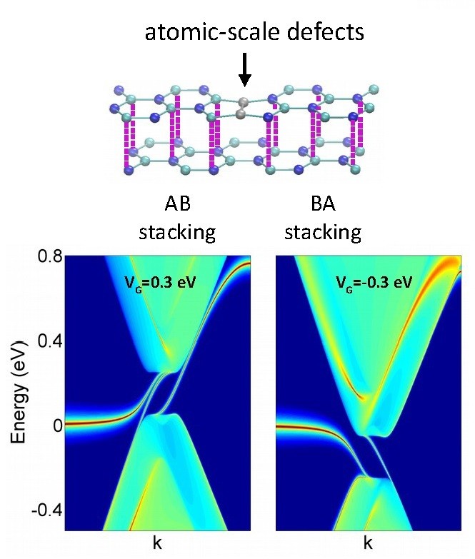 Bilayer graphene having a boundary with a change of stacking from AB to BA built by a defect line in the top layer. (a) Structural model. Atoms are colored in cyan and blue following the A and B sublattices, respectively. The nodes in grey color are mixing the two sublattices. Local density of states as a function of energy and wavevector along the defect line, for gate voltages either (c) positive V=0.3 eV or (d) negative V=-0.3 eV. Note that due to gate voltage polarization, the number of gap states is assymetric.