Giant tunnelling electroresistance in atomic-scale ferroelectric tunnel junctions for non-volatile memories
- The collaborative team, led by Rui Yang from the University of Michigan-Shanghai Jiao Tong University Joint Institute, Linxing Zhang from Beijing University of Science and Technology, and Yue-Wen Fang from CFM, reported the construction of nanoscale ferroelectric tunnel junctions. These 1 nm junctions achieved a giant tunnelling electroresistance of 700,000, setting a new record for resistance ratio in ferroelectric tunnel junctions at atomic-scale thicknesses. The 4 nm tunnel juctions even show higher performance than commercial flash.
Ferroelectric tunnel junctions (FTJs) hold promise for the next generation of high-reliability, low-power non-volatile storage and in-memory computing devices due to their small size, excellent repeatability, and low read/write energy consumption. The ferroelectric thin film allows the quantum mechanical tunneling of electrons, with the average tunneling barrier and thus the tunneling electroresistance (TER) modulated by the polarization of the ferroelectric layer. Generally, the high TER of ferroelectric tunnel junctions is advantageous for reducing power consumption and improving the stability of devices. However, maintaining a high TER is challenging with the decreased thickness of the ferroelectric tunneling layer.
Guided by crystal structure design, the team has previously achieved robust room-temperature ferroelectricity in 1 nm samarium-doped bismuth oxide (BSO) thin films (DOI: 10.1126/science.abm5134). Based on these thin films, this work proposes FTJs of Au/Cr/BSO/NSTO where NSTO refers to niobium-doped strontium titanate (see Fig. 1). This junction structure significantly improves the on/off ratio because both barrier height and width are modulated upon the polarization reversal. For the FTJs with ferroelectric layer thickness as low as 1 nm, a giant TER exceeding 700,000 has been achieved, representing an improvement of over three orders of magnitude compared to same-thickness devices in previous studies. Moreover, as the thickness of the film increases, the TER of the devices can be further enhanced, with the highest TER exceeding one billion obtained in the FTJs with a ferroelectric layer thickness of 4.6 nm, which is higher than commercial flash memories.
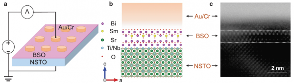
Figure 1. The structure of ferroelectric tunnel junction in this work.
In addition, by varying the reset stop voltages, 32 distinct resistance states (5 bits of data storage) are realized in a single FTJ, implying the multi-level information storage can be realized in such devices. Moreover, the devices demonstrate linear conductance modulation, more than five billion endurance cycles, and over 10 years of retention time (see Fig. 2). These BSO-based FTJs hold high promise towards reliable, high-performance, high-density and low-power non-volatile memory and in-memory computing applications.
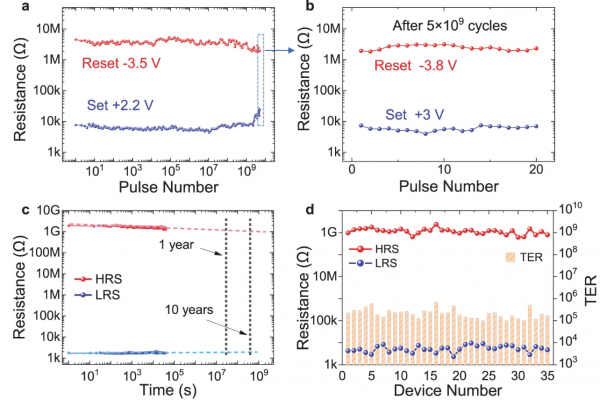
Figure 2. (a) Measured endurance properties showing more than five billion cycles under +2.2 V/−3.5 V programming pulses. (b) high-resistance state (HRS) and low-resistance state (LRS) after five billion programming cycles, showing that the device can maintain robust tunneling electroresistance (TER) effect by applying slightly larger programming voltages. (c) Measured retention property showing that TER over 100,000 can be maintained for more than 10 years. (d) HRS, LRS, and TER measured for 35 devices, showing small device-to-device variation.