Modelling Light Emission From Tunnelling Nanojunctions
The tunnelling current established between two metallic electrodes at a nanojunction induces light emission, a not-yet-fully-understood process that can be leveraged to design novel sources of light. A unified description is developed that describes the light emission induced by inelastic processes in the entire nanojunction, including the metal electrodes.
Original publication: Unified Treatment of Light Emission by Inelastic Tunneling: Interaction of Electrons and Photons beyond the Gap.
A voltage applied at a junction formed by two metal electrodes separated by an insulator nanogap induces a continuous tunnelling current when the gap separation is small enough, of the order of a few nanometers. This continuous current can then lead to the emission of light at optical frequencies, as experimentally demonstrated.
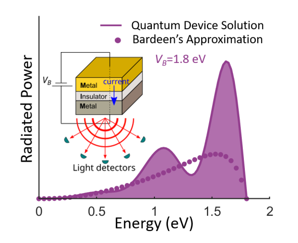
Figure. Example of the spectrum of the light generated by a tunnelling current flowing through the sketched nanojunction. The results obtained with the Quantum Device Solution developed in this work predict much more light emission than Bardeen’s approximation, an alternative approach that only consider the generation of photons by inelastic processes in the insulator nanogap.
A first explanation of light emission from the tunnelling junction considers inelastic tunnelling processes occurring in the insulator nanogap. However, recent experiments measure stronger emission than predicted by this model, a finding that can be assigned to the action of an alternative mechanism, the generation of hot charges at the metal itself.
In this work, performed by the “Theory of Nanophotonics” group at the Centro de Física de Materiales and the Donostia International Physics Center in San Sebastián, together with Prof. Jean-Jacques Greffet at the Institut d’Optique Graduate School in France, a unifying theoretical model of the light emission process is developed, the Quantum Device Solution (QDS). The QDS describes, within a single unified framework, the generation of photons by inelastic tunnelling processes occurring both at the insulator nanogap and at the metal electrodes, without invoking hot charge generation as a separate mechanism of light emission. The QDS also establishes the equivalence of the two previous descriptions of photon generation by inelastic tunnelling processes in the insulator nanogap, which considered either Fermi’s golden rule or the excitation of resonant modes by quantum fluctuations of the current.
The predictions of the QDS, evaluated for a configuration of metallic layers of current experimental interest, show that under certain conditions more light is expected to be emitted when the inelastic processes at the metal electrodes are taken into account. The possibility of a strong additional increase of the emitted light due to non-local effects is also explored. The QDS can thus guide the design of novel light sources based on photon emission induced by tunnelling currents in nanojunctions, and could be extended to describe the statistical properties of the emitted light.