Native point defects and their implications for the Dirac point gap at MnBi2Te4(0001)
Recently discovered antiferromagnetic topological insulator MnBi2Te4 represents a fertile platform for realization of numerous quantum phenomena. The characteristic making this material so attractive is its predicted large surface gap. This study reveals an unexpected and dramatic negative effect that MnBi2Te4’s native defects may have on the size of this g
The size of the surface gap of MnBi2Te4 has been a subject of a fierce debate recently. Density functional theory calculations predict this gap to reach almost 100 meV. However, the experimental studies have reported contradictory results, with some groups finding a gapped surface, in agreement with theoretical predictions, while others revealing practically gapless spectrum. A number of possible theoretical explanations of this unexpected behavior have been put forward, but none of them has been confirmed experimentally.
In this paper, the authors report on a combined study of the MnBi2Te4(0001) surface using low-temperature scanning tunneling microscopy/spectroscopy (STM/S), high-resolution micro(μ)-laser angle-resolved photoemission spectroscopy (ARPES), and density functional theory calculations. High-resolution STM topographs complemented by the STM simulations allow the team to identify a presence of an intermixing between Mn and Bi sublattices of the material (Fig. 1a). The appearance of the Mn-Bi intermixing causes deviations of the magnetic structure from the ideal antiferromagnetic to a ferromagnetic one, in which the local moments of the MnBi defects are coupled antiparallel to those of the central Mn layer. The STS measurements further reveal that, depending on the sample cleavage, the local density of states is compatible with both large (~50 meV) and small (<20 meV) gaps (Fig. 1c,e), in agreement with the laser-ARPES experiments, detecting that the gap changes from sample to sample (Fig. 1b,d).
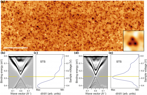
Figure 1 (a) STM image of a representative area where the characteristic second layer defects (MnBi) indicative of the Mn-Bi intermixing can be observed (1 V and 0.1 nA, scale bar 25 nm). Inset: Zoom of 2.5 nm2 of one of the MnBi defects taken at 1 V and 0.1 nA. (b, d) Measured MnBi2Te4(0001) ARPES dispersions corresponding to a larger (b) and smaller (d) gaps (measurements conditions: photon energy hν = 6.3 eV; temperature T = 10 K). Note that the second-derivative (d2N/dE2) representation of the photoemission data is shown. (c, e) Spatially averaged tunneling conductance spectra showing a clear dip (c) and peak (e) at the expected energy position of the gap center. The spectra shown in (c, e) are compatible with larger (~50 meV) and smaller (<20 meV) gaps, respectively. The horizontal yellow lines show the correspondence between the ARPES and STS spectra. The ARPES data in (b) and (d) correspond to two different samples, while the STS data in (c) and (e) have been acquired from yet another sample, but after different cleavages.
These surface electronic structure calculations show that the MnBi defects cause a strong reduction of the MnBi2Te4 surface gap due to the antiparallel alignment of the MnBi moments with respect to those of the Mn layer and predominant localization of the topological surface state near the Bi layers (Fig. 2). We thus attribute the variation of the surface gap in the same sample (as observed by STS) or different samples (ARPES) to a different degree of the defectness of the MnBi2Te4 crystals at local or global structure level, respectively. These results are instrumental in unifying seemingly contradictory reports concerning the MnBi2Te4 surface gap and stress a necessity of suppressing the cation (Mn-Bi) intermixing thus reducing the number of the MnBi defects in this antiferromagnetic topological insulator.
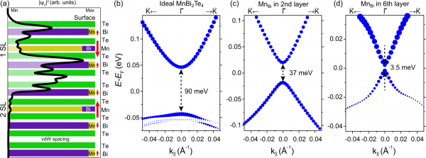
Figure 2 (a) Illustration of the topological surface state real space distribution at the MnBi2Te4(0001) surface. The ∣Ψz∣2 profile corresponds to the band structure shown in panel (b). The Mn-Bi intermixing leads to the appearance of the MnBi magnetic moments in the Bi layers that are coupled antiparallel to those in the central Mn layer of the same septuple layer (SL). The MnBi magnetic moments thus turn out to be located in the regions with a high weight of the topological surface state, strongly counteracting the effect from the magnetization of the central Mn layer, where the topological surface state weight is low. This is expected to lead to a strong reduction of the surface gap. The latter is illustrated in panels (b–d), where the MnBi2Te4 surface electronic structure in the defectless case (b) is compared to those with Mn-Bi intermixing when MnBi defect locates in the second (c) and sixth (d) atomic (i.e., Bi) layers counting from the surface (see (a)). Note that only the topological surface state is shown, while the bulk-like bands are omitted. The energy axes scales in (b, c) and (d) are different.