Quantum Transport Revealed in Optics: Plasmonic Response of Metallic Nanojunctions Driven by Single Atom Motion
Can individual atoms drive Optics? This seems difficult since the wavelength of visible light is thousands of times larger than the typical atomic dimensions. However, with the promise of molecular electronic devices, closing this length-scale gap has become a key, open issue in the search for novel electro-optical devices. Plasmons are known for their ability to localize light down to the nanometer scale. Unfortunately, this is still at least one order of magnitude larger than the typical atomic size. In this communication, the group showed that the distribution of local fields around metal nanoparticles is affected by their structure at the atomic scale. However, the optical response in the far field is usually quite insensitive to such details. Thus, the question arises whether this can be done better. Can the rearrangement of a few atoms influence the plasmonic response of a nanometer-scale object in a way that can be measured by optical means?
The modelization and simulation group at CFM gives an affirmative answer to these questions. The conclusions driven by the results stem obtained from a theoretical analysis of the properties of a plasmonic cavity (see the Figure below) formed by two nanoparticles, a canonical model for tip-enhanced spectroscopy set-ups. These calculations are possible thanks to the efficient implementation of linear response theory within the framework of time-dependent density functional theory (TDDFT). The researchers observe the spontaneous formation of ultrathin metal necks across a metal nanojunction, which features quantized electron transport. Due to this quantization, changes of the contact cross-section involving just one atom give rise to discontinuous, abrupt changes in the current. In this work, it is demonstrated that such quantized current jumps translate into sudden changes of the intensities, spectral positions and widths of the cavity plasmon resonances. The simulations are not a mere theoretical “divertimento”. Nanocontacts similar to those described in our report but made out of gold, a prototypical plasmonic material, have been already fabricated and studied in experimental laboratories worldwide.
Thus, these results indicate that the far-field optical response of nanometer-sized objects can be tuned by structural rearrangements involving a few or even a single atom, opening new avenues for research of active control devices in Nanoptics.
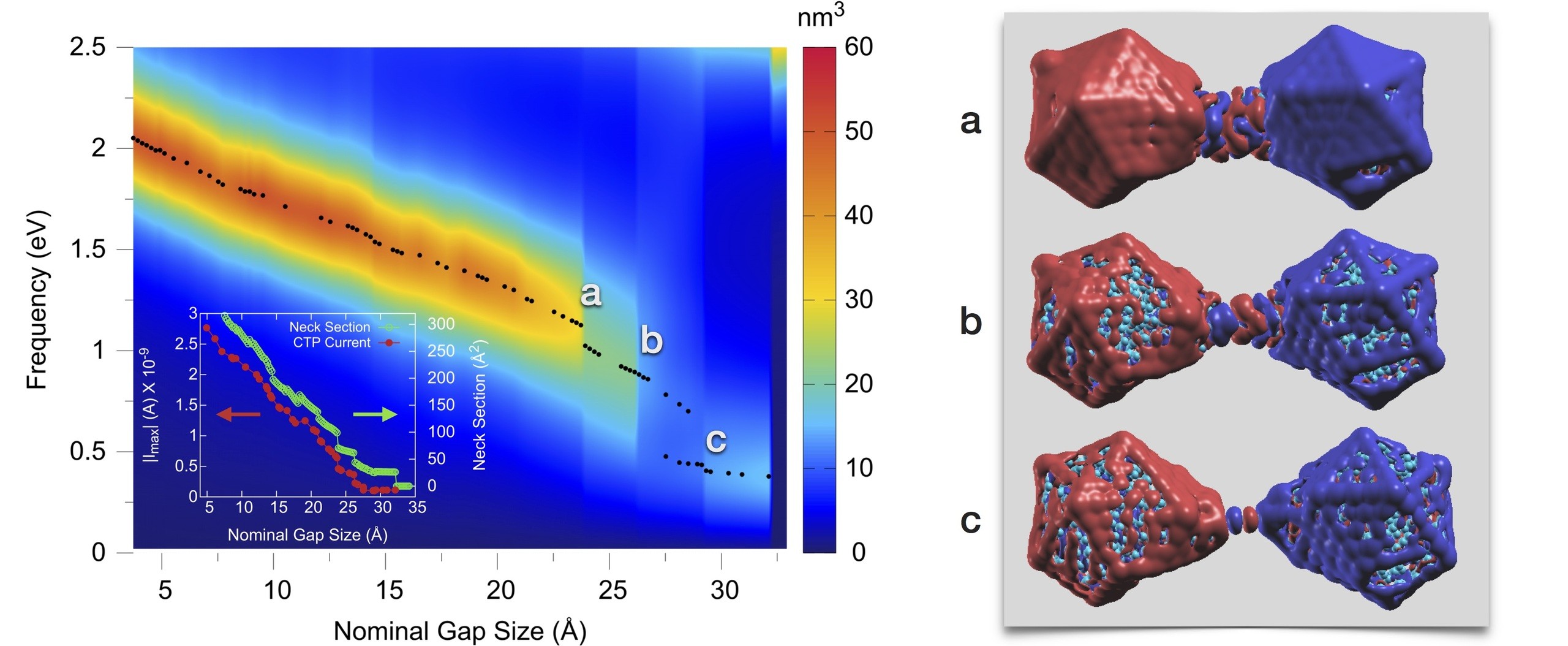
Left panel: Evolution of the resonances in the imaginary part of the polarizability as a function of the junction size. Due to the spontaneous formation of a metal neck across the nanojunction, we can observe a characteristic charge-transfer plasmon (CTP) mode all the way up to ~30 Å nominal separations between the particles. The inset shows the electric current flowing through the junction (at the frequency of the CTP resonance), and the evolution of the cross-section of the neck. There is a one-to-one correspondence between the jumps observed in the current, in the neck cross-section and in the far-field optical response of the plasmonic cavity. Right panels: Structure of the system formed by Na380 particles at the separations indicated as (a), (b) and (c) in the left panel. Imaginary part of the induced electronic charge distribution at the CTP resonance frequency for each of the configurations is also plotted (different colors indicate charge accumulation and charge depletion).