TOWARDS TUNABLE CHARGE CARRIER INJECTION BARRIERS AT DONOR-ACCEPTOR/METAL INTERFACES
Semiconductor-electrode interfaces are among the key elements in charge injection devices. In the case of a model system comprising archetypical planar semiconducting molecules and atomically flat metal substrates, it can be generally defined by a monolayer-thick blend of donor and acceptor molecules in contact with the metal surface.
Energy barriers for hole and electron injection are determined by the offset from the highest occupied molecular orbital (HOMO) and lowest unoccupied molecular orbital (LUMO) of this contact layer with respect to the Fermi level of the metal electrode. However, the HOMO and LUMO alignment is not easy to elucidate in complex multi-component, molecular/metal systems. In addition, it is not well understood how the interface energetics depend on the different supramolecular environments comparing single component layers with molecular blends. Here we demonstrate that core-level photoemission from donor-acceptor/metal interfaces can straightforwardly and transparently assess molecular level alignment. Systematic experiments in a variety of systems show a characteristic binding energy shift in core-levels as a function of molecular donor/acceptor ratio, irrespectively of the molecule or the metal.
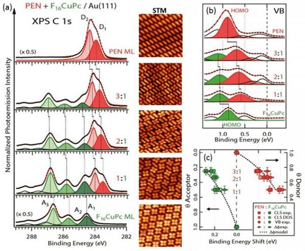
In particular, donor levels shift to lower binding energies, whereas acceptor levels shift to higher binding energies. This is exemplified in Figure 1 for the case of pentacene (PEN, donor) and fluorinated copper-phthalocyanines (F16CuPc, acceptor) on Au(111) surfaces. The C 1s core level spectra associated with each of the crystalline structures as a function of molecular stoichiometry are displayed in Fig. 1a, evidencing a rigid shift of all the different components. The same shift is observed in the molecular orbitals, as displayed in Fig. 1b for the respective HOMO levels, and inferred from X-ray absorption spectroscopy (NEXAFS) measurements for the LUMO levels. Interestingly, all these shifts could be reproduced with density functional theory calculations and follow a stoichiometry dependent change in the system’s work function (Fig. 1c) in a local vacuum-level pinning scenario. The blend’s work function can be further estimated by averaging that of the single component layers, weighted by the partial-coverage of each of the molecules (Fig. 1c).
Our findings therefore demonstrate the possibility to assess interface energetics by core level photoemission, greatly facilitating the characterization of donor-acceptor blends on electrode surfaces. Furthermore, they open a route to tune critical parameters for the efficiency of devices, as are the charge injection barriers at metal-organic interfaces. The interface dipoles associated with donor and acceptor molecules can differ significantly, allowing a substantial range over which to tune the system’s work function by the blend stoichiometry in a predictable manner. With this work we therefore don’t only advance in the understanding, but also provide a handle for the control of charge injection barriers in technologically relevant donor-acceptor/metal interfaces.
1Centro de Fisica de Materiales CSIC/UPV, Spain, 2Departamento de Fisica Aplicada I, Universidad del Pais Vasco, San Sebastian, Spain, 3Donostia International Physics Center, San Sebastian, Spain, 4CNR-IOM, Centro Nazionale TASC, Bassovizza, Italy, 5Nano-Bio Spectroscopy Group and ETSF Scientific Development Center, Departamento de Fisica de Materiales, Universidad del Pais Vasco UPV/EHU, San Sebastian, Spain, 6National Institute for Materials Science, Tsukuba, Japan, 7Department of Physics, University of California at Berkeley, United States.