Ultrafast electronic response of graphene to a strong and localized electric field
New experiments and simulations have shown that it is possible for extremely high currents to pass through graphene. This allows imbalances in electric charge to be rapidly rectified without introducing any damage in the graphene layer.
An international research team, formed by both theorists (CFM-UPV/EHU and DIPC, Donostia, and CNRS, Paris) and experimentalists (Helmholtz-Center, Dresden-Rossendorf, University of Duisburg-Essen and TU, Wien), was able to prove that electrons in graphene are extremely mobile and react very quickly to an ultrahigh electric field. In the experiments, xenon ions, with a particularly high electric charge, impact on a graphene single layer film producing a large number of electrons to be torn away from the graphene in a very precise spot. However, thanks to the theoretical simulations, it was possible to understand that the material is able to replace the electrons within some femtoseconds. This resulted in extremely high currents, which would not be maintained under normal circumstances. Its extraordinary electronic properties make graphene a very promising candidate for future applications in the field of electronics.
The highly charged Xe ions used in the experiments have initial positive charges up to +35, which means that 35 electrons have been removed in the ion source before it collides with the graphene film. However, as it is approaching the film it starts tearing electrons away from the graphene due to its extremely strong electric field. By the time the ion has fully passed through the graphene layer, it has a positive charge of less than +10, compared to over +30 when it started out. The ion is able to extract more than 20 electrons from a tiny area of the graphene film. This means that electrons are now missing from the graphene layer, so the carbon atoms surrounding the point of impact of the xenon ions are positively charged.
The group´s simulations using time dependent density functional theory (TDDFT) reveal the highly non-linear multielectron processes responsible for the ultrafast response (few femtoseconds) of graphene electrons to the extremely high electric field produced by the highly charged ion. These processes take place in a few nanometers size spot of the graphene layer, something that translates into extremely high current densities both in the perpendicular and transverse directions to the graphene plane, as shown in the figure below. Additionally, the team show that the experimentally measured keV energy loss experienced by the highly charged ion is transferred to electronic degrees of freedom. Mainly the energy is taken away by ionization of several tens of electrons into the continuum. The holes left in a nm size graphene area as a result of an electron emission and electron capture by the projectile are so quickly neutralized that there is no time to transfer the energy to the lattice producing structural defects.
This extremely high electron mobility in graphene is of great significance for a number of potential applications, like the construction of ultrafast electronic devices or connecting optical and electronic components.
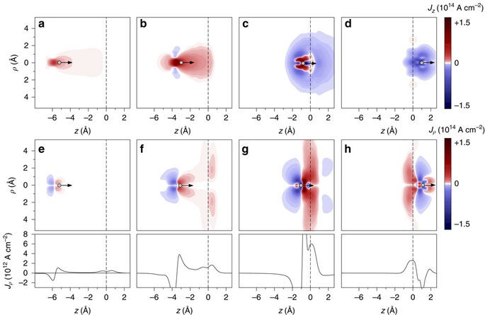 Snapshots of the perpendicular Jz (a–d) and radial Jρ (e–h) components of the current density for qin=20 at four different HCI–graphene distances obtained from TDDFT calculations performed in cylindrical (ρ,z) coordinates with z-axis set along the projectile trajectory perpendicular to the target surface. The figures show that already above the graphene layer electrons are transferred to the approaching HCI and the current density along the direction of motion explains the charge exchange of the HCI. Extremely high transverse current density (f–h) along the graphene layer is obtained. The corresponding profiles (lower panels) show the z-dependent transverse current density averaged over a circle of 10 Å in radius. Values exceeding 1012 A cm−2 are obtained. The position of the HCI is indicated by a small circle, while the position of the graphene layer by the vertical dashed line.