Visualizing 1D topological edge states with atomic resolution

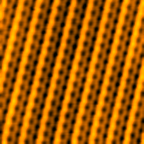
Atomically resolved STM image of the 1T’ phase in WSe2.
In 2007 a new kind of materials termed “topological insulators” was discovered. These materials are technologically relevant because are insulating in their interior but can support the flow of electrons on their boundaries. Furthermore, these electronic states are robust, maintained even in the presence of defects, which creates new opportunities for dissipationless electronics. Although a large number of 3D topological insulators have been discovered since 2007, the scarce 2D topological insulators that have so far been confirmed are mostly complex heterostructures with limited potential for technological applications. This has created an urgent need for finding more practical, large-gap 2D topological insulators.
Written in Nature Communications, Miguel M. Ugeda (CFM-DIPC) and his colleagues from UC Berkeley (USA), Stanford University (USA) and Ecole Polytechnique Fédérale de Lausanne (EPFL) (Switzerland) report the experimental evidence that the structural 1T’ phase of a single layer of WSe2 – a 2D material – is a topological insulator. The work presents experimental evidence of band inversion, a large gap opening of 120 meV and the electronic edge state formation in single-layer 1T’-WSe2, all of them signature characteristics of topological insulators. Furthermore, the researchers were able to visualize with atomic resolution the characteristic topologically protected electronic states at the edge of the 1T’ phase and measure its characteristic penetration length, a critical parameter in topological insulator. The demonstration that the 1T’ phase of WSe2 is a true 2D topological insulator is a breakthrough in the field of nanotechnology since it is a material that is stable in its isolated, 2D form without the need of a special substrate. This will enable the realization of topological-based 2D flexible devices that exploit dissipationless charge and spin transport.


